Results
Graphitization
|
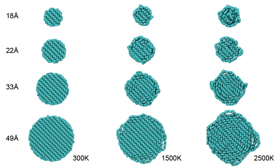
Simulation runs investigating the graphitization of spherical nanodiamonds clearly show that this process can be numerically described using the Tersoff potential in good agreement with experimental data. A dependency of the graphitization velocity on simulation temperature and a dependency of the degree of graphitization on nanodiamond size were found.
Figure 2 shows snapshots from relevant simulations of nanodiamonds with different diameters. On the left, the simulation temperature was set to 300K, in the middle it was set to 1500K and on the right the simulation temperature was 2500K. First signs of graphitization at the surface can be seen for the 1500K case, whereas at 2500K all structures are almost completely turned into so-called onion-ring structures.
Implantation
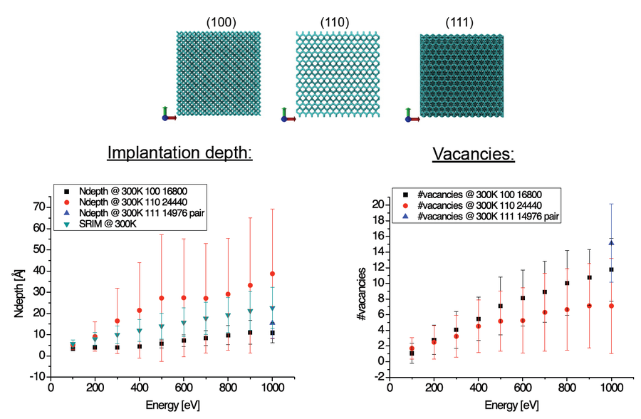
First successful low energy (<1keV) implantation runs examined and confirmed the validity and the applicability of simulations with the ITAP molecular dynamic (IMD) package to diamond systems. A combination of the Tersoff- and the Ziegler-Biersack-Littmark-potential was used to describe the interactions between atoms. The results clearly show the influence of crystal orientation, temperature and implantation energy on both the depth distribution of implanted nitrogen and the number of created vacancies.
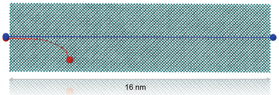
Based on experimentally executed implantations concerning shallow NV center production 4keV implantations were simulated and analyzed via specifically developed tools. In this way the channeling effect after implantation in the (100) plane was obtained (see Figures 3, 4 and 5). This effect was suppressed by a 7° tilting of the implantation angle, in agreement with experimental findings. Furthermore, differences in implantation results were extracted by using different projectiles (N and N2). Here the total number and the distribution of created vacancies as well as the distance between nitrogen atoms were under investigation.
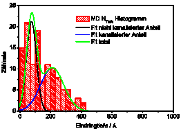
Figure 5 shows the nitrogen depth distribution after 4keV implantation using IMD. 2 maxima can be observed: Nitrogen atoms which stopped closer to the surface are considered as “not channeled” whereas nitrogen atoms which penetrated deeper into the crystal are identified as “channeled”.
|
|
|
Annealing
A basic requirement for the creation of optical usable NV centers is their structural arrangement. The defect consists of a carbon atom which is replaced by a nitrogen atom together with an adjacent vacancy. Generally after the implantation process vacancy and nitrogen atom are not next neighbors. Therefore, in experiments, diamonds are heated up to temperatures of 900-1000K over several hours (annealing). Thus, vacancies are mobile and become trapped by fixed nitrogen atoms. This configuration is thermally stable. Previous experiments have shown that shallow nitrogen implantations (<10keV) result in a low NV− yield of 0.01−0.1%.
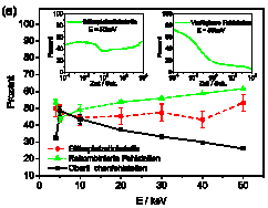
The aim of our investigation was to study the dynamics of defects during the annealing process. Therefore a specifically Monte Carlo (MC) code was introduced. The simulations consider the main drain processes resulting in a reduction of the final NV yield: Vacancies which are lost to the surface, recombinations of vacancies with interstitial atoms, thermally stable defects containing nitrogen atoms and formation of vacancy clusters as well as an interchange of positions between nitrogen atoms placed on a lattice site with interstitial carbon atoms. In the MC code previously calculated activation energies are used for the migration of defects in the carbon matrix. Figure 6 shows the results of annealing after a 2h simulation.
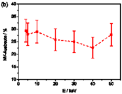
The insets in Figure 6 show the evolution of nitrogen atoms placed on a lattice site after 2h of annealing (left) and the vacancies available to form NV centers over simulation time (right). The main graph describes the main processes leading to a reduction of the final NV yield. The main graph on the right shows final NV yield results depending on the implantation energy. We observed a nearly constant NV yield of 25% in the implantation energy range of 4-50keV. This result is significantly higher than the NV yield seen in earlier experimental publications. An explanation of the discrepancy can be given by surface effects or damage structure in the vicinity of shallow NV centers which are not recovered after annealing.
|
|
|
Optical investigations
For a broad range of applications built on NV centers, it is necessary to control the charge state of the system. Using ab-initio calculation techniques, we obtained a mechanism for transforming a negatively charged NV center (NV-) into a neutral (NV0) and vice versa (see Figure 7).

- Fig. 7: Schematic illustration of transformation from NV- to NV0 (a) and vice versa (b).
The photoionization involves two steps: The absorption of two photons followed by an auger process.
Thanks to its outstanding optical properties another defect in diamond shifts into the focus of research: The negatively charged silicon-vacancy center (SiV center). This color center shows in particular optical stable fluorescence for diamond sizes of ~2nm. In contrast, the smallest diamonds containing stable optical NV defects were not found experimentally for system smaller than ~8nm in diameter. In the course of this, we investigated hydrogen passivated diamonds with embedded SiV centers. In particular, we calculated the Zero-Phonon-Line (ZPL), which describes the emission energy of a system in the excited state after previously an electron of an occupied spin down state eu was excited into an unoccupied spin down state eg (see Figure 8). Our results clearly show a quantum confinement effect on the excitation spectrum. This effect changes the valance band maximum (VBM). In bulk material the eu level is energetically in the valance band and shifts into the bandgap with decreasing diamond size. This leads to a reduction of exchange and correlation interaction between bandgap and other electrons. As a consequence, the electron states in the bandgap split energetically.
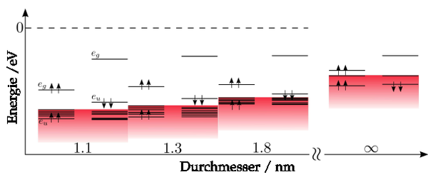
- Fig. 8: Energy level diagram for the SiV defect embedded in diamond depending on system size.


